Detailed Device Info
Note: "SPI connector" is now referred to as "wireless add-on port."
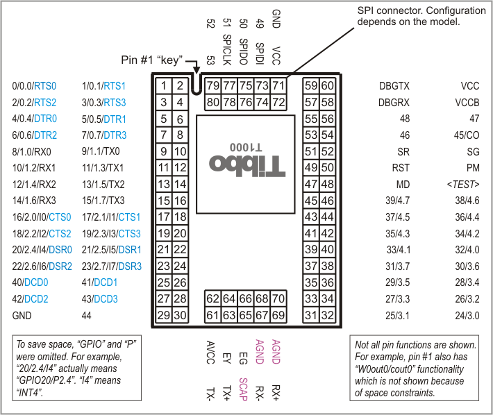
I/O Pin Assignment
|
Pin # |
Function |
Description |
|
1(1,2) |
GPIO0/P0.0 |
General-purpose I/O line 0 (P0.0). |
|
2(1,2) |
GPIO1/P0.1 |
General-purpose I/O line 1 (P0.1). |
|
3(1,2) |
GPIO2/P0.2 |
General-purpose I/O line 2 (P0.2). |
|
4(1,2) |
GPIO3/P0.3 |
General-purpose I/O line 3 (P0.3). |
|
5(1,2) |
GPIO4/P0.4 |
General-purpose I/O line 4 (P0.4). |
|
6(1,2) |
GPIO5/P0.5 |
General-purpose I/O line 5 (P0.5). |
|
7(1,2) |
GPIO6/P0.6 |
General-purpose I/O line 6 (P0.6). |
|
8(1,2) |
GPIO7/P0.7 |
General-purpose I/O line 7 (P0.7). |
|
9(1,2) |
GPIO8/P1.0/RX0 |
General-purpose I/O line 8 (P1.0); RX, W1, and din input of the serial port 0. |
|
10(1,2) |
GPIO9/P1.1/TX0 |
General-purpose I/O line 9 (P1.1); TX, W1, and dout output of the serial port 0. |
|
11(1,2) |
GPIO10/P1.2/RX1 |
General-purpose I/O line 10 (P1.2); RX, W1, and din input of the serial port 1. |
|
12(1,2) |
GPIO11/P1.3/TX1 |
General-purpose I/O line 11 (P1.3); TX, W1, and dout output of the serial port 1. |
|
13(1,2) |
GPIO12/P1.4/RX2 |
General-purpose I/O line 12 (P1.4); RX, W1, and din input of the serial port 2. |
|
14(1,2) |
GPIO13/P1.5/TX2 |
General-purpose I/O line 13 (P1.5); TX, W1, and dout output of the serial port 2. |
|
15(1,2) |
GPIO14/P1.6/RX3 |
General-purpose I/O line 14 (P1.6); RX, W1, and din input of the serial port 3. |
|
16(1,2) |
GPIO15/P1.7/TX3 |
General-purpose I/O line 15 (P1.7); TX, W1, and dout output of the serial port 3. |
|
17(1,2,3) |
GPIO16/P2.0/INT0 |
General-purpose I/O line 16 (P2.0); interrupt line 0. |
|
18(1,2,3) |
GPIO17/P2.1/INT1 |
General-purpose I/O line 17 (P2.1); interrupt line 1. |
|
19(1,2,3) |
GPIO18/P2.2/INT2 |
General-purpose I/O line 18 (P2.2); interrupt line 2. |
|
20(1,2,3) |
GPIO19/P2.3/INT3 |
General-purpose I/O line 19 (P2.3); interrupt line 3. |
|
21(1,2,3) |
GPIO20/P2.4/INT4 |
General-purpose I/O line 20 (P2.4); interrupt line 4. |
|
22(1,2,3) |
GPIO21/P2.5/INT5 |
General-purpose I/O line 21 (P2.5); interrupt line 5. |
|
23(1,2,3) |
GPIO22/P2.6/INT6 |
General-purpose I/O line 22 (P2.6); interrupt line 6. |
|
24(1,2,3) |
GPIO23/P2.7/INT7 |
General-purpose I/O line 23 (P2.7); interrupt line 7. |
|
25(1,2) |
GPIO40 |
General-purpose I/O line 40 (does not belong to any 8-bit port). |
|
26(1,2) |
GPIO41 |
General-purpose I/O line 41 (does not belong to any 8-bit port). |
|
27(1,2) |
GPIO42 |
General-purpose I/O line 42 (does not belong to any 8-bit port). |
|
28(1,2) |
GPIO43 |
General-purpose I/O line 43 (does not belong to any 8-bit port). |
|
29 |
GND |
System ground. |
|
30(1,2) |
GPIO44 |
General-purpose I/O line 44. |
|
31(1,2) |
GPIO25/P3.1 |
General-purpose I/O line 25 (P3.1). |
|
32(1,2) |
GPIO24/P3.0 |
General-purpose I/O line 24 (P3.0). |
|
33(1,2) |
GPIO27/P3.3 |
General-purpose I/O line 27 (P3.3). |
|
34 (1,2) |
GPIO26/P3.2 |
General-purpose I/O line 26 (P3.2). |
|
35(1,2) |
GPIO29/P3.5 |
General-purpose I/O line 29 (P3.5). |
|
36(1,2) |
GPIO28/P3.4 |
General-purpose I/O line 28 (P3.4). |
|
37(1,2) |
GPIO31/P3.7 |
General-purpose I/O line 31 (P3.7). |
|
38(1,2) |
GPIO30/P3.6 |
General-purpose I/O line 30 (P3.6). |
|
39(1,2) |
GPIO33/P4.1 |
General-purpose I/O line 33 (P4.1). |
|
40(1,2) |
GPIO32/P4.0 |
General-purpose I/O line 32 (P4.0). |
|
41(1,2) |
GPIO35/P4.3 |
General-purpose I/O line 35 (P4.3). |
|
42(1,2) |
GPIO34/P4.2 |
General-purpose I/O line 34 (P4.2). |
|
43(1,2) |
GPIO37/P4.5 |
General-purpose I/O line 37 (P4.5). |
|
44(1,2) |
GPIO36/P4.4 |
General-purpose I/O line 36 (P4.4). |
|
45(1,2) |
GPIO39/P4.7 |
General-purpose I/O line 39 (P4.7). |
|
46(1,2) |
GPIO38/P4.6 |
General-purpose I/O line 38 (P4.6). |
|
47 |
MD |
Mode selection pin. |
|
48 |
<TEST PIN> |
Leave this pin unconnected. |
|
49 |
RST |
Reset line, active high. |
|
50 |
PM |
PLL control line (HIGH- PLL ON, LOW- PLL OFF). |
|
51 |
SR |
Red status LED control line. |
|
52 |
SG |
Green status LED control line. |
|
53(1,2) |
GPIO46 |
General-purpose I/O line 46. |
|
54(1,2) |
GPIO45/CO |
General-purpose I/O line 45 (does not belong to any 8-bit port); square wave output line. |
|
55(1,2) |
GPIO48 |
General-purpose I/O line 48 (does not belong to any 8-bit port). |
|
56(1,2) |
GPIO47 |
General-purpose I/O line 47 (does not belong to any 8-bit port). |
|
57 |
DBGRX |
RX line of debug serial port (details to be published). |
|
58 |
VCCB |
Backup power for the real-time counter; connect to 3.3V through a 50 Ohm resistor. |
|
59 |
DBGTX |
TX line of debug serial port (details to be published). |
|
60 |
VCC |
Positive power input, 3.3V nominal, +/- 5%, max. current consumption 230mA (100BaseT, PLL on). |
|
61 |
TX- |
Ethernet port, negative line of the differential output signal pair. |
|
62 |
AVCC |
"Clean" power output for magnetics circuitry: EM1000-...-00: 3.3V (not in production) EM1000-...-01/-02: 2.5V (currently in production). |
|
63 |
TX+ |
Ethernet port, positive line of the differential output signal pair. |
|
64 |
EY |
Yellow Ethernet status LED control line. |
|
65 |
EM1000-...- 00: --- EM1000-...- 01: SCAP |
EM1000-...-00: --- EM1000-...-01/-02: external supercapacitor input. |
|
66 |
EG |
Green Ethernet status LED control line. |
|
67 |
RX- |
Ethernet port, negative line of the differential input signal pair. |
|
68 |
EM1000-...- 00: --- EM1000-...- 01: AGND |
EM1000-...-00: --- EM1000-...-01/-02: analog ground. |
|
69 |
RX+ |
Ethernet port, positive line of the differential input signal pair. |
|
70 |
EM1000-...- 00: --- EM1000-...- 01: AGND |
EM1000-...-00: --- EM1000-...-01/-02: analog ground. |
|
71(4) |
GND |
System ground. |
|
72(4) |
VCC |
3.3V power available on this pin. Do not connect to the power source. To avoid current loops, only use pin #60 to power the device. |
|
73(1,2,4) |
GPIO49 |
General-purpose I/O line 49 (does not belong to any 8-bit port). |
|
74(4,5) |
SPIDI |
SPI, data in [no longer in use]. |
|
75(1,2,4) |
GPIO50 |
General-purpose I/O line 50 (does not belong to any 8-bit port). |
|
76(4,5) |
SPIDO |
SPI, data out [no longer in use]. |
|
77(1,2,4) |
GPIO51 |
General-purpose I/O line 51 (does not belong to any 8-bit port). |
|
78(1,2,4,5) |
SPICLK |
SPI, clock line [no longer in use]. |
|
79(1,2,4) |
GPIO52 |
General-purpose I/O line 52 (does not belong to any 8-bit port). |
|
80(1,2,4) |
GPIO53 |
General-purpose I/O line 53 (does not belong to any 8-bit port). |
- This line is 5V-tolerant and can be interfaced to 5V CMOS devices directly.
- This line can be mapped to serve as an RTS/Wout/cout line of a serial port (provided that this does not interfere with any other function).
- This line can serve as a CTS/W0&1in/cin line of a serial port (provided that this does not interfere with any other function).
- This pin is on the wireless add-on port (formerly known as "SPI port"). The "-A" option devices have the connector header soldered in and "available" to the host PCB. "T" option devices have a female connector. Other EM1000 versions do not have any connector installed.
- The SPI lines are no longer used. Our current wireless add-on modules, such as the WA2000, rely on GPIO49~53 for communicating with add-on devices. SPIDI, SPIDO, and SPOCLK lines should never be connected.
Additional Resources
See these topics for more information on various hardware facilities of the EM1000:
- General-Purpose I/O Lines
- Wireless Add-On Port
- Ethernet Port Lines
- Serial Ports
- Square Wave Generator
- Flash Memory and EEPROM
- Real-Time Counter
- LED Lines
- Power, Reset, PLL Control, and Mode Selection Lines