A/D Converter
The A/D converter is based on Analog Devices' 24-bit AD7712 chip and has eight independent channels.
Each channel has two differential input lines. The maximum input range is ±10V. The range can be adjusted to 1/2, 1/4, ... 1/128 of that by programming the internal gain of the A/D circuit to 2, 4, ...128. With a gain of 1 and bipolar mode selected, applying +10V to the A/D input produces the conversion result of "all 1's." Applying –10V produces "all 0's." Applying 0V produces "1" followed by 0's (this is a "middle" value). Of course, this explanation is idealized, as it doesn't take into account inevitable conversion errors.
The A/D converter is designed for relatively slow, but highly accurate measurements. With the recommended configuration (see below), the converter will produce 250 measurements/second for any selected channel. Only one channel can be selected at any given time.
The A/D converter has full galvanic isolation from the rest of the IB1004 + SB1004 circuitry: The power for the A/D section is generated by an isolated switching power supply; all control lines use opto-couplers.
A/D Inputs
The A/D converter inputs are available on terminal blocks 1 and 2.
Terminal Block 1:
|
Terminal # |
Function |
|
9 |
A/D channel 4, negative input (–) |
|
8 |
A/D channel 4, positive input (+) |
|
7 |
A/D channel 3, negative input (–) |
|
6 |
A/D channel 3, positive input (+) |
|
5 |
A/D channel 2, negative input (–) |
|
4 |
A/D channel 2, positive input (+) |
|
3 |
A/D channel 1, negative input (–) |
|
2 |
A/D channel 1, positive input (+) |
|
1 |
A/D ground (isolated from the rest of the device) |
Terminal Block 2:
|
Terminal # |
Function |
|
9 |
A/D channel 8, negative input (–) |
|
8 |
A/D channel 8, positive input (+) |
|
7 |
A/D channel 7, negative input (–) |
|
6 |
A/D channel 7, positive input (+) |
|
5 |
A/D channel 6, negative input (–) |
|
4 |
A/D channel 6, positive input (+) |
|
3 |
A/D channel 5, negative input (–) |
|
2 |
A/D channel 5, positive input (+) |
|
1 |
A/D ground (isolated from the rest of the device) |
A/D Control Lines
Nine lines of the EM1000 (located on the NB10x0 network board) control the A/D converter. In the table below, "output" means an output of the EM1000 and "input" means an input of the EM1000:
|
Line |
Function |
Corresponding EM1000 I/O line |
IC1000 cable line |
|
DO (output) |
Serial data out |
GPIO13 |
27 |
|
DI (input) |
Serial data in |
GPIO12 |
25 |
|
CLOCK (output) |
Serial clock (LOW idle state) |
GPIO2 |
5 |
|
C/D (output) |
Register selection:
|
GPIO40 |
6 |
|
RFS (output) |
Receive frame sync (active LOW) |
GPIO32 |
30 |
|
TFS (output) |
Transmit frame sync (active LOW) |
GPIO33 |
28 |
|
CHS0 (output) |
Channel selection, bit 0 |
GPIO41 |
8 |
|
CHS1 (output) |
Channel selection, bit 1 |
GPIO42 |
10 |
|
CHS2 (output) |
Channel selection, bit 2 |
GPIO43 |
12 |
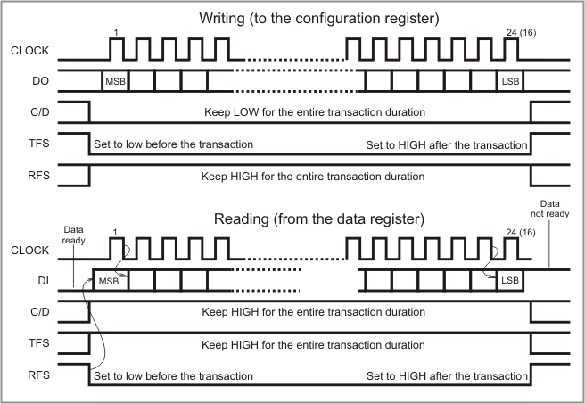
The A/D converter has a 24-bit configuration register and a 24-bit data register that contains the A/D conversion result. These registers are accessed through the serial interface consisting of five I/O lines:
- Two lines — RFS and TFS — are used for selecting the transaction type. The inactive state for these signals is HIGH. The RFS line must be set LOW prior to the read transaction and remain LOW for the entire transaction duration. The TFS line must be set LOW prior to the write transaction and remain LOW for the entire transaction duration.
- The CLOCK line is used both for writing to and reading from the converter. The inactive state for this line is LOW. Each read and write "transaction" consists of 24 clock pulses, after which the clock returns to the LOW state. Alternatively, the IC can be programmed for 16-bit resolution, in which case each transaction will consist of 16 pulses.
- The DO line is for sending the data to the converter (writing to the configuration register). Each data bit must be placed on the DO line while the CLOCK is LOW. This means that the first, most significant bit, of data must be placed on the DO line before the first clock pulse of the transaction. Switching the CLOCK from LOW to HIGH will latch the bit into the converter.
- The DI line serves double purposes. Before the RFS line is brought LOW, the DI input indicates whether new measurement data is ready. The DI line is HIGH while the converter is not ready and goes LOW when the new data becomes available. After the RFS line is brought LOW, the DI is used to receive the data from the converter (read the data register). The most significant bit of the readout is present on the DI line right after the RFS becomes LOW. The converter will output next data bit on every HIGH to LOW transition on the CLOCK line. We recommend that your application records the data while the CLOCK line is HIGH.
- The C/D line defines whether the data is exchanged with the configuration register (C/D is LOW), or data register that contains the conversion result (C/D is HIGH). The C/D line must remain stable (HIGH or LOW) for the entire duration of the transaction.
Read and write "transactions" are illustrated in the diagram below.
The A/D converter has eight inputs and three control lines — CHS2, CHS1, and CHS0 — are used to select the channel. Only one channel can be selected at any given time.
Preparing to Communicate With the A/D Converter
Before you start exchanging data with the A/D converter you need to configure certain GPIO lines of the EM1000 as outputs. These lines are CLOCK, DO, C/D, TFS, RFS, CHS0, CHS1, and CHS2. In other words, all lines except DI must be configured as outputs.
Writing to the Configuration Register
Follow these steps to write to the configuration register:
- Set the C/D line LOW to indicate that the configuration register access will take place.
- Set the TFS line LOW to indicate that this will be a write operation (RFS must remain HIGH).
- Place the value of the most significant bit of the configuration word on the DO line.
- Set the CLOCK line HIGH.
- Set the CLOCK line LOW. This will conclude the first clock pulse.
- Generate 23 additional clock pulses, every time setting the next bit on the DO line while the CLOCK is at LOW.
- Set the TFS line HIGH. The write is complete.
A/D Converter Initialization
If you refer to the data sheet for the AD7712 you will find that there are many configuration options. Without resorting to reprinting the data sheet, we provide the following brief info:
|
bit23 |
bit22 |
bit21 |
bit20 |
bit19 |
bit18 |
bit17 |
bit16 |
bit15 |
bit14 |
bit13 |
bit12 |
|
MD2 |
MD1 |
MD0 |
G2 |
G1 |
G0 |
CH |
PD |
WL |
X |
BO |
BU |
|
bit11 |
bit10 |
bit9 |
bit8 |
bit7 |
bit6 |
bit5 |
bit4 |
bit3 |
bit2 |
bit1 |
bit0 |
|
FS11 |
FS10 |
FS9 |
FS8 |
FS7 |
FS6 |
FS5 |
FS4 |
FS3 |
FS2 |
FS1 |
FS0 |
- The MD2-0 field is set to 000 for normal operation or 001 for self-calibration. There are also other configuration modes available, but they are not supported by the IB1004.
- The G2-0 field defines the gain of the A/D. The signal measured by the A/D is pre-amplified according to this gain. Writing 000 will select the gain of 1, 001 the gain of 2, ... 111 the gain of 128.
- The CH field selects the channel and has to be set to 1 for the IB1004 to work properly. This channel selection should not be confused with the IB1004 input channel selector described above.
- The PD power down bit should be at 0.
- The WL word length bit should be at 0 for 16-bit resolution (sufficient for most applications), or at 1 for 24-bit resolution.
- The BO burnout current bit should be at 0.
- The B/U bit should be at 0 to select bipolar operation.
- The FS11-0 filter selection bits that should be set according to the requirements of your application. We often use the value of 4E Hex. Read page 10 of the IC's datasheet and you will find out that this corresponds with the data rate of 250Hz (times/second) and the effective resolution of 15 bits. We choose this as a good compromise between the speed and resolution. We choose the resolution of 15 bits because the D/A portion of the product has the resolution of 14 bits.
To initialize the A/D converter, write the desired configuration word on startup. For the 15-bit effective resolution described above write the hex value of 22004E. This will set up the converter and kick-off a self-calibration process (see below).
Optional Self-Calibration
The A/D converter will operate at a better precision if you calibrate it first. Set bits MD2-0 of the configuration register to 001 to start self-calibration. Self-calibration, as the name implies, is an automatic process that does not require any external intervention. The calibration takes time. To determine when the calibration is over, poll the DI line after writing to the configuration register:
- Once the TFS line goes HIGH marking the end of the write transaction, the DI line starts indicating the status of the converter.
- The DI line will be HIGH while the converter is still busy.
- The DI line will become LOW when the calibration is finished.
There is no need to set MD2-0 = 000 after the calibration — this happens automatically. So, in effect, your entire A/D converter setup may consist of writing 22004E hex (or other suitable configuration word) and waiting for the DI to become LOW.
Changing Channels
Follow these steps to change the channel:
- If the desired channel is not selected yet, select it by manipulating control lines CHS2-0. Code 000 selects the channel 1, 001 channel 2, ... 111 channel 8.
- After the channel change, discard the results of the first conversion. This is because the channel change may result in the wrong measurement. The second measurement will contain correct data. Alternatively, your program can wait the time equal to two A/D measurement periods. Conversion period is related to the filter setting. For the filter set at 250Hz, the conversion period is 1/250Hz = 4ms. So, the application needs to wait for 8ms before correct data for the newly selected channel becomes available.
Receiving A/D Conversion Result
The data register of the A/D converter is updated at the conversion rate (for our recommended setting, 1/250Hz = 4ms). So, the new measurement result is available every 4ms. You are always reading the most recent conversion result.
The readout can only start when the A/D converter is ready. Starting the read transaction when the converter is not ready will produce invalid data (you will read "all zeroes" or "all ones"). Follow this algorithm to perform the read:
- While the RFS line is at HIGH, read the state of the DI line. If the line is HIGH, then the A/D converter is not ready and you need to wait.
- Keep polling the DI line until it becomes LOW. This will indicate that the read transaction can be started.
- Set C/D line HIGH to indicate that the data register access will take place.
- Set the RFS line LOW to indicate that this will be a read operation (TFS must remain HIGH).
- Set the CLOCK line HIGH and record the state of the DI line — this is the value of the most significant bit.
- Set the CLOCK LOW — this concludes the first clock cycle.
- Perform 23 or 15 more clock cycles (depending on the value you set in the WL bit of the configuration register), every time recording the state of the DI line when the CLOCK is it HIGH.
- Set the RFS line HIGH. The read is complete.
 Remember that the "effective resolution" discussed above has nothing to do with the number of bits you are supposed to read from the converter. This number is either 24 or 16, depending on the WL bit of the configuration register.
Clock Speed Limitations
The A/D converter is optically isolated from the rest of the device, so there are opto-couplers on all interface lines. Opto-couplers are relatively slow devices. This imposes a limit on how fast the clock line can be toggled. The minimum clock period is 200µs. Both half-periods must be at least 100µs long. This means that the conversion result can be obtained in 200µs * 24 = 4.8ms or 200µs * 16 = 3.2ms.