Detailed Device Info
Note: "SPI connector" is now referred to as "wireless add-on port"
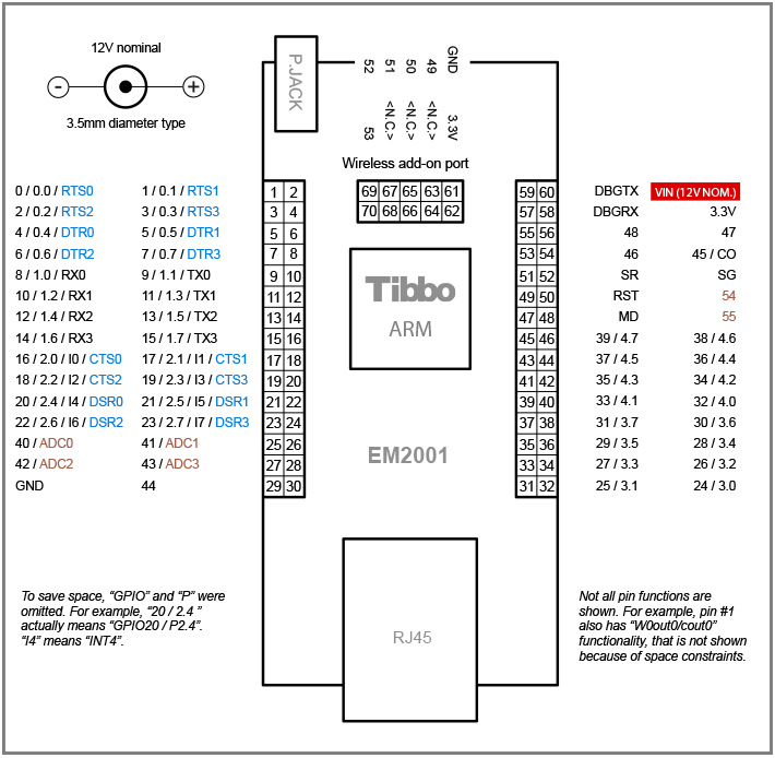
I/O Pin Assignment
|
Pin # |
Function |
Description |
|
1(1,2) |
GPIO0/P0.0/RTS0 |
General-purpose I/O line 0 (P0.0). |
|
2(1,2) |
GPIO1/P0.1/RTS1 |
General-purpose I/O line 1 (P0.1). |
|
3(1,2) |
GPIO2/P0.2/RTS2 |
General-purpose I/O line 2 (P0.2). |
|
4(1,2) |
GPIO3/P0.3/RTS3 |
General-purpose I/O line 3 (P0.3). |
|
5(1,2) |
GPIO4/P0.4/DTR0 |
General-purpose I/O line 4 (P0.4). |
|
6(1,2) |
GPIO5/P0.5/DTR1 |
General-purpose I/O line 5 (P0.5). |
|
7(1,2) |
GPIO6/P0.6/DTR2 |
General-purpose I/O line 6 (P0.6). |
|
8(1,2) |
GPIO7/P0.7/DTR3 |
General-purpose I/O line 7 (P0.7). |
|
9(1,2) |
GPIO8/P1.0/RX0 |
General-purpose I/O line 8 (P1.0); RX, W1 input, and din input of serial port 0. |
|
10(1,2) |
GPIO9/P1.1/TX0 |
General-purpose I/O line 9 (P1.1); TX, W1 output, and dout output of serial port 0. |
|
11(1,2) |
GPIO10/P1.2/RX1 |
General-purpose I/O line 10 (P1.2); RX, W1 input, and din input of serial port 1. |
|
12(1,2) |
GPIO11/P1.3/TX1 |
General-purpose I/O line 11 (P1.3); TX, W1 output, and dout output of serial port 1. |
|
13(1,2) |
GPIO12/P1.4/RX2 |
General-purpose I/O line 12 (P1.4); RX, W1 input, and din input of serial port 2. |
|
14(1,2) |
GPIO13/P1.5/TX2 |
General-purpose I/O line 13 (P1.5); TX, W1 output, and dout output of serial port 2. |
|
15(1,2) |
GPIO14/P1.6/RX3 |
General-purpose I/O line 14 (P1.6); RX, W1 input, and din input of serial port 3. |
|
16(1,2) |
GPIO15/P1.7/TX3 |
General-purpose I/O line 15 (P1.7); TX, W1 output, and dout output of serial port 3. |
|
17(1,2,3) |
GPIO16/P2.0/INT0/CTS0 |
General-purpose I/O line 16 (P2.0); interrupt line 0. |
|
18(1,2,3) |
GPIO17/P2.1/INT1/CTS1 |
General-purpose I/O line 17 (P2.1); interrupt line 1. |
|
19(1,2,3) |
GPIO18/P2.2/INT2/CTS2 |
General-purpose I/O line 18 (P2.2); interrupt line 2. |
|
20(1,2,3) |
GPIO19/P2.3/INT3/CTS3 |
General-purpose I/O line 19 (P2.3); interrupt line 3. |
|
21(1,2,3) |
GPIO20/P2.4/INT4/DSR0 |
General-purpose I/O line 20 (P2.4); interrupt line 4. |
|
22(1,2,3) |
GPIO21/P2.5/INT5/DSR1 |
General-purpose I/O line 21 (P2.5); interrupt line 5. |
|
23(1,2,3) |
GPIO22/P2.6/INT6/DSR2 |
General-purpose I/O line 22 (P2.6); interrupt line 6. |
|
24(1,2,3) |
GPIO23/P2.7/INT7/DSR3 |
General-purpose I/O line 23 (P2.7); interrupt line 7. |
|
25(1,2) |
GPIO40/ADC0 |
General-purpose I/O line 40 (does not belong to any 8-bit port); ADC input 0. |
|
26(1,2) |
GPIO41/ADC1 |
General-purpose I/O line 41 (does not belong to any 8-bit port); ADC input 1. |
|
27(1,2) |
GPIO42/ADC2 |
General-purpose I/O line 42 (does not belong to any 8-bit port); ADC input 2. |
|
28(1,2) |
GPIO43/ADC3 |
General-purpose I/O line 43 (does not belong to any 8-bit port); ADC input 3. |
|
29 |
GND |
System ground. |
|
30(1,2) |
GPIO44 |
General-purpose I/O line 44 (does not belong to any 8-bit port). |
|
31(1,2) |
GPIO25/P3.1 |
General-purpose I/O line 25 (P3.1). |
|
32(1,2) |
GPIO24/P3.0 |
General-purpose I/O line 24 (P3.0). |
|
33(1,2) |
GPIO27/P3.3 |
General-purpose I/O line 27 (P3.3). |
|
34(1,2) |
GPIO26/P3.2 |
General-purpose I/O line 26 (P3.2). |
|
35(1,2) |
GPIO29/P3.5 |
General-purpose I/O line 29 (P3.5). |
|
36(1,2) |
GPIO28/P3.4 |
General-purpose I/O line 28 (P3.4). |
|
37(1,2) |
GPIO31/P3.7 |
General-purpose I/O line 31 (P3.7). |
|
38(1,2) |
GPIO30/P3.6 |
General-purpose I/O line 30 (P3.6). |
|
39(1,2) |
GPIO33/P4.1 |
General-purpose I/O line 33 (P4.1). |
|
40(1,2) |
GPIO32/P4.0 |
General-purpose I/O line 32 (P4.0). |
|
41(1,2) |
GPIO35/P4.3 |
General-purpose I/O line 35 (P4.3). |
|
42(1,2) |
GPIO34/P4.2 |
General-purpose I/O line 34 (P4.2). |
|
43(1,2) |
GPIO37/P4.5 |
General-purpose I/O line 37 (P4.5). |
|
44(1,2) |
GPIO36/P4.4 |
General-purpose I/O line 36 (P4.4). |
|
45(1,2) |
GPIO39/P4.7 |
General-purpose I/O line 39 (P4.7). |
|
46(1,2) |
GPIO38/P4.6 |
General-purpose I/O line 38 (P4.6). |
|
47 |
MD |
Mode selection pin. |
|
48(1,2) |
GPIO55 |
General-purpose I/O line 55 (does not belong to any 8-bit port). |
|
49 |
RST |
Reset line, active low. |
|
50(1,2) |
GPIO54 |
General-purpose I/O line 54 (does not belong to any 8-bit port). |
|
51 |
SR |
Red status LED control line. |
|
52 |
SG |
Green status LED control line. |
|
53(1,2) |
GPIO46 |
General-purpose I/O line 46. |
|
54(1,2) |
GPIO45/CO |
General-purpose I/O line 45 (does not belong to any 8-bit port); square wave output line. |
|
55(1,2) |
GPIO48 |
General-purpose I/O line 48 (does not belong to any 8-bit port). |
|
56(1,2) |
GPIO47 |
General-purpose I/O line 47 (does not belong to any 8-bit port). |
|
57 |
DBGRX |
RX line of debug serial port. |
|
58 |
3.3V |
Direct 3.3V power input or 3.3V power output if you are supplying 12V power via a power jack or VIN pin. |
|
59 |
DBGTX |
TX line of debug serial port. |
|
60 |
VIN (12V NOM.) |
12V (nominal) power input to the onboard power regulator. Acceptable input voltage range is 8V~20V. |
|
61 |
GND |
Wireless add-on port, ground line. |
|
62 |
VCC |
Wireless add-on port, 3.3V power output for the wireless add-on module. |
|
63(1,2) |
GPIO49 |
Wireless add-on port, general-purpose I/O line 49 (does not belong to any 8-bit port). |
|
64 |
<N.C.> |
Leave this pin unconnected. |
|
65(1,2) |
GPIO50 |
Wireless add-on port, general-purpose I/O line 50 (does not belong to any 8-bit port). |
|
66 |
<N.C.> |
Leave this pin unconnected. |
|
67(1,2) |
GPIO51 |
Wireless add-on port, general-purpose I/O line 51 (does not belong to any 8-bit port). |
|
68 |
<N.C.> |
Leave this pin unconnected. |
|
69(1,2) |
GPIO52 |
Wireless add-on port, general-purpose I/O line 52 (does not belong to any 8-bit port). |
|
70(1,2) |
GPIO53 |
Wireless add-on port, general-purpose I/O line 53 (does not belong to any 8-bit port). |
- This line is 5V-tolerant and can be interfaced to 5V CMOS devices directly.
- This line can be mapped to serve as an RTS, W0 output, or CLOCK output line of a serial port. The line can also be assigned to an I²C/SPI channel, or act as an interface line of the Wi-Fi add-on module, keypad, or an LED control channel.
- This line can serve as a CTS, W0&1 input, or CLOCK input line of a serial port.
Additional Resources
See these topics for more information on various hardware facilities of the EM2001:
- General-Purpose I/O Lines
- Wireless Add-On Port, Wi-Fi Communications
- Ethernet Port
- Serial Ports
- Analog-to-Digital Converter (ADC)
- I²C/SPI Support (SSI Channels)
- Square Wave Generator
- Flash Memory and EEPROM
- Real-Time Clock (RTC) and Backup Battery
- LEDs and LED Lines
- External LCD Support
- External Keypad Support
- Power, Reset, PLL Control, and Mode Selection Lines